egais registers. When should balances in egais be equal to actual balances? Transfer of products to the second register Does not completely transfer to the 2nd register 1c
7.2 Transfer registers
7.2.1 FIFO Violation Event Register (FWEV)
| bit 7 RXFIFO3 |
bit 6 RXFIFO2 |
bit 5 RXFIFO1 |
bit 4 - |
bit 3 TXFIFO3 |
bit 2 TXFIFO2 |
bit 1 TXFIFO1 |
bit 0 - |
| RXWARN3-1 | Reserved | TXWARN3-1 | Reserved | ||||
| 0 | 0 | 0 | - | 0 | 0 | 0 | - |
| r | - | r | - | ||||
TXWARN. Transmission disruption warning. Set to "1" when the corresponding transmitting FIFO endpoint has exceeded the limit defined by the TFWL bit in the TXCx register and transmission from the corresponding endpoint is enabled. This bit is cleared when the violation warning condition is cleared, either by writing new data to the FIFO when the FIFO is cleared, or upon completion of the transfer, as indicated by the TX_DONE bit in the TXSx register.
RXWARN. Reception warning. Set to "1" when the corresponding transmitting FIFO endpoint has exceeded the limit specified by the RFWL bit in the EPCx register. This bit is cleared when the violation warning condition is cleared, either by reading data from the FIFO or when the FIFO is cleared.
7.2.2 FIFO Violation Mask Register (FWMSK)
When the corresponding bit in the FWEV register is set, WARN in the MAEV register is set. When cleared, the corresponding bit in the FWEV register does not cause WARN to be set.
| bit 7 | bit 6 | bit 5 | bit 4 | bit 3 | bit 2 | bit 1 | bit 0 |
| Same bit description as in FWEV register | |||||||
| 0 | 0 | 0 | 0 | 0 | 0 | 0 | 0 |
| r/w | |||||||
7.2.3 Frame Number Significant Register (FNH)
| bit 7 | bit 6 | bit 5 | bit 4 | bit 3 | bit 2 | bit 1 | bit 0 |
| M.F. | UL | RFC | Reserved | FN10-8 | |||
| 1 | 1 | 0 | - | 0 | 0 | 0 | |
| r | r | w/r | - | r | |||
FN. Frame number. This is the current received frame number in the last SOF packet. If the correct frame number is not received during the 12060 bits (maximum frame length, FLMAX) of the previous exchange, then the frame number is artificially increased. If two consecutive frames are missed or incorrect, the current FN is frozen and loaded with the frame number from the SOF packet.
If the low byte of the frame number was read by the firmware before reading the FNH register, then the user is actually reading the contents of the buffer register, which contains the value of the three frame number bits of that register when the low byte was read. The correct sequence to read the frame number is: FNL, FNH. Read operations for the FNH register, without first reading the Frame Number Low Byte (FNL) register, read the actual value of the three least significant bits into the frame number. Upon reset, FN is set to "0".
RFC. Reset frame counter. Setting this bit resets the frame number to 0x0000, after which this bit clears itself. This bit is always read as "0".
UL. Unlock flag. This bit indicates that at least two frames were received without the expected frame number, or that a valid SOF was not received within 12060 bits of arrival time. If this bit is set, then the frame number from the next valid packet is loaded into the FN. When reset, this flag is set to "1".
M.F. Lost SOF flag. This bit is set when the frame number in the received SOF packet is not equal to the expected value, or when SOF is not received within 12060 bits of arrival time. When reset, this flag is set to "1".
7.2.4 Frame Number Low Byte Register (FNL)
This register contains the low byte of the frame number, as described above. To ensure consistency, reading this low byte causes the three frame number bits in the FNH register to be latched while the register is read. The correct sequence for reading the frame number is: FNL, FNH. Upon reset, FN is set to "0".
| bit 7 | bit 6 | bit 5 | bit 4 | bit 3 | bit 2 | bit 1 | bit 0 |
| FN7-0 | |||||||
| 0 | 0 | 0 | 0 | 0 | 0 | 0 | 0 |
| r | |||||||
7.2.5 Functional Address Register (FAR)
This register sets the functional address of the device. The different endpoint numbers are set individually via the endpoint control register.
| bit 7 | bit 6 | bit 5 | bit 4 | bit 3 | bit 2 | bit 1 | bit 0 |
| AD_EN | AD6-0 | ||||||
| 0 | 0 | 0 | 0 | 0 | 0 | 0 | 0 |
| r/w | r/w | ||||||
A.D. Address. This field contains the 7-bit functional address used to send and receive all characters addressed to the device.
AD_EN. Addressing resolution. When the bit is set to "1", bits AD6-0 are used in address comparison (see Section 6.2 for details). When cleared, the device does not respond to any character on the bus.
Note: If the DEF bit in the checkpoint 0 control register is set, then endpoint 0 responds to its default address.
7.2.6 DMA Control Register (DMACNTRL)
| bit 7 | bit 6 | bit 5 | bit 4 | bit 3 | bit 2 | bit 1 | bit 0 |
| DEN | IGNRXTGL | DTGL | ADMA | DMOD | DSRC2-0 | ||
| 0 | 0 | 0 | 0 | 0 | 0 | - | 0 |
| r/w | r/w | r/w | r/w | r/w | r/w | ||
DSRC. DMA source. The DMA Source bits field contains a binary value that determines which of the endpoints, 1...6, are available to support DMA. DSRC bits are cleared on reset. Table 7 shows the DSRC bit settings.
Table 7. Description of DSRC bits
| DSRC | Endpoint number | ||
| 2 | 1 | 0 | |
| 0 | 0 | 0 | 1 |
| 0 | 0 | 1 | 2 |
| 0 | 1 | 0 | 3 |
| 0 | 1 | 1 | 4 |
| 1 | 0 | 0 | 5 |
| 1 | 0 | 1 | 6 |
| 1 | 1 | x | Reserved |
DMOD. DMA mode. This bit determines when a DMA request occurs. If it is cleared, the DMA request appears when the transfer is completed. For transmitting endpoints EP1, EP3 and EP5, the data is fully transmitted, as indicated by the TX_DONE bit (to fill the FIFO with new transmitted data). For receiving endpoints EP2, EP4 and EP6, this is reflected by the RX_LAST bit. When the DMOD bit is set, a DMA request occurs when the corresponding FIFO violation warning bit is set. The DMOD bit is cleared on reset.
The DMA request from the sending endpoint is activated until the request state is cleared. If DMOD is set to "0", then DMA requests occur either until the firmware reads the corresponding transmit status register (TXSx), thereby clearing the TX_DONE bit, or if the TX_LAST bit in the transmit command register (TXCx) installed by hardware-implemented software. If the DMOD bit is set to "1", then DMA requests occur until FIFO violation warning states caused by either sending enough bytes to the endpoint or if the TX_DONE bit is set due to a transfer are cleared.
The DMA request from the sending endpoint is activated until the request state is cleared. If DMOD is set to "0", then DMA requests occur either until the firmware reads the corresponding receive status register (RXSx), thereby clearing the RX_LAST bit, or if the FIFO becomes empty due to enough cycles reading. If the DMOD bit is set to "1", then DMA requests occur until the FIFO violation warning states are cleared or the FIFO endpoint becomes empty due to enough read cycles.
If DMOD is set to "0" and the endpoint and DMA are enabled, then a DMA request occurs as long as the firmware reads the corresponding TXSx or RXSx register, thereby clearing the TX_DONE/RX_LAST bit. If the DMOD bit is set to "1" and the endpoint and DMA are enabled, then the DMA request occurs as long as the FIFO violation alert states.
ADMA. Automatic DMA. Setting this bit automatically enables the selected receive or transmit endpoint. Before enabling ADMA mode, the DEN bit in the DMA Control Register (DMACNTRL) must be cleared. ADMA mode operates as long as any bit other than NTGL in the DMA Event Register (DMAEV) is set. To initialize ADMA mode, all bits except NTGL in the DMAEV register must be cleared.
For receive operations, the receiver is turned on automatically; When a packet is received, it is transferred via DMA to memory.
For transfer operations, the data packet is sent via DMA from memory; the transmitter turns on automatically.
When a device enters ADMA mode, any existing endpoint state may be lost. If there is already data in the FIFO, it is reset. The current state of RX_EN and TX_EN may also change.
Clearing ADMA takes the device out of ADMA mode. DEN may clear at the same time or later. If at the same time, then all DMA operations stop immediately and the firmware must send any remaining data. If later, the device will complete any current DMA operation before exiting ADMA mode (see the description of the DSHL bit in the DMAEV register).
DTGL. DMA switch. This bit is used to determine the status of ADMA operations upon initialization. During initialization, the firmware sets this bit to "1" if it starts with a DATA1 operation, and to "0" if it starts with a DATA0 operation.
Writing this bit also updates the NTGL bit in the DMAEV register.
IGNRXTGL. Ignoring RX switching. If this bit is set, the comparison between the NTGL bit in the DMAEV register and the TOGGLE bit in the corresponding RXSx register is ignored during receive operations. In this case, a mismatch of both bits during a receive operation will not stop the ADMA operation. If this bit is not set, ADMA stops if there is a bit mismatch. After reset, this bit is set to "0".
7.2.7 DMA Event Register (DMAEV)
The bits in this register are used in ADMA mode. Bits 0...3 may cause an interrupt if they are not cleared, even if the device has not set ADMA mode. Until all these bits are cleared, ADMA mode cannot be initialized. ADMA mode automatically ends when any of these bits are set.
| bit 7 | bit 6 | bit 5 | bit 4 | bit 3 | bit 2 | bit 1 | bit 0 |
| Reserved | NTGL | Reserved | DSIZ | DCNT | DERR | DSHLT | |
| - | 0 | - | 0 | 0 | - | 0 | |
| - | r | - | CoW | CoW | CoW | CoW | |
DSHLT. DMA software stop. This bit is set when ADMA operations are stopped by firmware. This bit is set only after the DMA engine has completed all necessary cleanup operations and returned to the idle state. Executed under the following conditions:
DERR. DMA error. This bit is set to indicate that the packet was received or sent incorrectly. It is also set if the TOGGLE bit in the RXSx/TXSx register is not equal to the NTGL bit in the DMAEV register after sending/receiving a packet. (Note that this comparison occurs before the NTGL bit changes state due to packet transmission.)
For receive, DERR is equivalent to RX_ERR. For transmission, it is equivalent to TX_DONE (set) and ACK_STAT (not set). If the AEH bit in the DMA Error Counter Register (DMAERR) is set, DERR will not be set until the DMAERRCNT in the DMAERR register is cleared and another error is detected. Errors are handled as specified in the DMAERR register.
DCNT. DMA counter. This bit is set when the DMA counter register (DMACNT) is "0" (see DMACNT register).
DSIZ. DMA size. This bit is only relevant for DMA receive operations. It indicates that the received packet is less than the full length of the FIFO. It usually indicates the end of a multi-packet transmission.
NTGL. Next switch. This bit determines the switching state when sending the next data packet (if sending), or the switching state when waiting for the next data packet (if receiving). This bit is initialized by writing the DTGL bit in the DMACNTRL register. It then changes state with each packet sent or received on the endpoint currently selected by DSRC2-0. If a DTGL write operation occurs at the same time as a bit update operation, the write operation has higher priority.
If a transfer occurs during ADMA operations, the DTGL bit overwrites the corresponding TOGGLE bit in the TXCx register. This ensures that the USB data is switched correctly.
Note that there are no corresponding mask bits for these events because they are not used to generate an interrupt.
7.2.8 DMA Mask Register (DMAMSK)
Any bit set to "1" in this register automatically sets the DMA bit in the ALTEV register when a corresponding event occurs in the DMAEV register. Otherwise, setting the DMA bit is disabled. For a description of bits 0…3, see the DMAEV register.
| bit 7 | bit 6 | bit 5 | bit 4 | bit 3 | bit 2 | bit 1 | bit 0 |
| DSIZ | DCNT | DERR | DSHLT | ||||
| - | 0 | 0 | - | 0 | |||
| - | r/w | r/w | r/w | r/w | |||
7.2.9 Mirror Register (MIR)
This register is read-only. Simply reading it does not change the state of the TXSx or RXSx register; the hardware-implemented software can freely check the state of the channel.
| bit 7 | bit 6 | bit 5 | bit 4 | bit 3 | bit 2 | bit 1 | bit 0 |
| STAT | |||||||
| - | |||||||
| r | |||||||
STAT. State. This field reflects the status bits of the transmitter or receiver selected in the DSRC2-0 field in the DMACNTRL register (DMA does not need to be active or enabled). It corresponds to TXSx or RXSx.
7.2.10 DMA Counter Register (DMACNT)
This register defines the maximum number specified for ADMA operations.
| bit 7 | bit 6 | bit 5 | bit 4 | bit 3 | bit 2 | bit 1 | bit 0 |
| AEH | DMAERRCNT | ||||||
| 0 | 0 | 0 | 0 | 0 | 0 | - | 0 |
| r/w | r/w | ||||||
DCOUNT. DMA counter. This field is decremented as a DMA operation completes until it becomes 0. The DCNT bit in the DMA event register is then set only when the next DMA operation completes successfully. This register does not lose significance.
For receive operations, this counter is decremented when a packet is successfully received and then transferred to memory via DMA.
For transfer operations, this counter is decremented when a packet is transferred from memory via DMA and then sent successfully.
DCOUNT should be set as follows: DCOUNT = (Packet No. to be sent) -1
If a DMACNT write operation occurs at the same time as a decrement operation, the write operation has higher priority.
7.2.11 DMA Error Register (DMAERR)
| bit 7 | bit 6 | bit 5 | bit 4 | bit 3 | bit 2 | bit 1 | bit 0 |
| FHT | H.O.S. | WKMODE | Reserved | ENUC | ENUSB | PNDUC | PNDUSB |
| 0 | 0 | 0 | - | 1 | 1 | 1 | 1 |
| w/r0 | w/r | w/r | - | w/r | w/r | CoW | CoW |
DMAERRCNT. DMA error counter. In conjunction with the arithmetic error handling capability, this counter determines the maximum number of consecutive bus errors before stopping ADMA mode. The hardware software can set the 7-bit counter to a preset value. Once ADMA is started, the counter is decremented by 1 from a preset value each time an error is detected on the bus. Each successful transition resets the counter back to the preset value. When ADMA mode is stopped, the counter is also set back to the preset value.
If the counter reaches 0 and another erroneous packet is detected, the DERR bit in the DMA event register is set. Details in section 7.2.7. This register does not lose significance.
DMAERRCNT should be set as follows: DMAERRCNT = 3D (Maximum number of send attempts attempted) - 1
Write access to this register is only possible when ADMA is inactive. Otherwise, it is ignored. Reading from this register while ADMA is active returns the current counter value. Reading from the register when ADMA is inactive returns the preset value. The counter is only decremented if AEH is set (automatic error handling activated).
Automatic error handling. This bit has two different meanings depending on the current transition mode:
This mode is used to transfer large arrays, interrupts and control. Setting AEH in this mode enables automatic processing of packets containing CRC or bit matching errors.
If this bit is set during transmit operations, the device automatically reloads the FIFO and requeues a packet for which the host controller did not return an ACK. If this bit is cleared, automatic error handling is disabled.
If this bit is set during receive operations, a packet received in error (as defined by the DERR bit in the DMAEV register) is automatically cleared from the FIFO to reacquire the packet. If this bit is cleared, automatic error handling is disabled.
Setting this bit allows the device to ignore packets received in error (as defined by the DERR bit in the DMAEV register).
If this bit is set during receive operations, the device automatically clears and resets the FIFO to receive the next packet. The erroneous packet is ignored and not sent through DMA. If this bit is cleared, automatic error handling is disabled.
7.2.12 Power-on register (WKUP)
| bit 7 | bit 6 | bit 5 | bit 4 | bit 3 | bit 2 | bit 1 | bit 0 |
| STALL | DEF | Reserved | EP3-0 | ||||
| 0 | 0 | - | 0 | 0 | 0 | 0 | 0 |
| r/w | r/w | - | r; hardware to "0" | ||||
PNDUSB. Expected USB enablement. This bit indicates that this device will be enabled by USB activity. It also sends a power-on wait interrupt request signal. The PNDUSB bit must be cleared by the host controller by writing "0". A hardware reset sets this bit.
PNDUC. Waiting for the microcontroller to turn on. This bit indicates that the device will be turned on when requested by the microcontroller. It also sends a power-on wait interrupt request signal. The PNDUC bit must be cleared by the host controller by writing "0". A hardware reset sets this bit.
ENUSB. USB resolution. When set to "1", this bit allows the device to turn on when USB activity is detected.
ENUC. Microcontroller resolution. When set to "1", this bit enables the device to turn on when the microcontroller accesses the device.
WKMODE. On mode. This bit selects the interval after which the device generates a power-up interrupt (if enabled) when a power-up event occurs, as shown below:
0 - Generates an immediate switch-on interrupt
1 - Generates a switch-on interrupt after a switch-on delay
HOS. Stop by suspension. When this bit is set, the device enters Halt mode as soon as it enters the suspend state. Writing a "1" in a suspended state has no effect.
FHT. Forced stop. When the node is not attached (NAT in the MCNTRL register is set to "0"), setting this bit puts the node into Halt mode. When the host is connected (NAT at "1"), the "1" entry is ignored.
7.2.13 Endpoint Control Register 0 (EPC0)
This register controls endpoint 0.
| bit 7 | bit 6 | bit 5 | bit 4 | bit 3 | bit 2 | bit 1 | bit 0 |
| Reserved | ACK_STAT | TX_DONE | TCOUNT4-0 | ||||
| - | 0 | 0 | 0 | 0 | 0 | 0 | 0 |
| - | CoR | CoR | r | ||||
EP. The end point. This field contains the 4-bit endpoint address. For endpoint 0, these bits are set to 0000b in hardware.
DEF. Default address. When this bit is set, the device responds to the default address, regardless of the contents of the FAR6-0/EP03-0 fields. When an IN character is sent for an endpoint, the DEF bit is automatically cleared.
This bit assists in the transition from the default address to the designated address. The transition from the default address 00000000000b to the address specified during bus numbering may fail in the middle of the SET_ADDRESS control sequence. This is necessary to complete the control sequence. However, the address must change immediately after the end of this sequence in order to avoid errors when another control sequence immediately follows the SET_ADRESS command.
On a USB reset, the firmware has 10 ms to set up, and must write 0x80 to the FAR register and 0x00 to the EPC0 register. Upon receipt of the SET_ADRESS command, the firmware must write 0x40 to the EPC0 register and 0x80 to the FAR register.
STALL.
1. - The transmit FIFO is enabled and the IN symbol is received.
2. - The receiving FIFO is enabled and an OUT character is received.
Note:
Upon transmission of confirmation of the STALL signal, the RX_LAST and TX_DONE bits are set in the corresponding transmit/receive status registers.
7.2.14 Transmission Status Register 0 (TXS0)
| bit 7 | bit 6 | bit 5 | bit 4 | bit 3 | bit 2 | bit 1 | bit 0 |
| Reserved | IGN_IN | FLUSH | TOGGLE | Reserved | TX_EN | ||
| - | 0 | 0 | 0 | 0 | 0 | - | 0 |
| - | r/w | r/w HW | r/w | - | r/w HW | ||
TCOUNT. Transfer counter. This bit indicates the number of empty bytes available in the FIFO. This field never exceeds 8 for endpoint 0.
TX_DONE. Transfer completed. When the bit is set, it indicates that the packet has been completely transmitted. It is cleared when this register is read.
ACK_STAT. Acknowledgment status. This bit indicates the status received from the main controller confirming the receipt of a previously sent packet. This bit is interpreted when TX_DONE is set to "1". It is set when an acknowledgment is received; otherwise, it remains purified. This bit is also cleared when this register is read.
7.2.15 Transmit Command Register 0 (TXC0)
| bit 7 | bit 6 | bit 5 | bit 4 | bit 3 | bit 2 | bit 1 | bit 0 |
| Reserved | IGN_IN | FLUSH | TOGGLE | Reserved | TX_EN | ||
| - | 0 | 0 | 0 | 0 | 0 | - | 0 |
| - | r/w | r/w HW | r/w | - | r/w HW | ||
TX_EN. Transfer permission. This bit enables data transfer from the FIFO. It is cleared by the chip after transmitting a single packet, or a STALL acknowledgment, in response to the IN symbol. It must be set by the firmware to begin transmitting the packet. The RX_EN bit in the Receive Command Register 0 (RXC0) takes precedence over this bit; because if RX_EN is set, the TX_EN bit is ignored until RX_EN is cleared.
Zero-length packets are shown when this bit is set without writing any FIFO data.
TOGGLE.
FLUSH. Writing a 1 to this bit clears all data from the control FIFO checkpoint, resets the endpoint to the Idle state, clears the FIFO read and write pointers, and then clears itself. If the endpoint is currently using FIFO0 to transfer data to USB, then the cleanup is delayed until the transfer completes. This bit is cleared on reset. It is equivalent to the FLUSH bit in register RXC0.
IGN_IN. Ignores the IN character. When this bit is set, the endpoint will ignore any IN character directed to its configured address.
7.2.16 Transmit Data Register 0 (TXD0)
| bit 7 | bit 6 | bit 5 | bit 4 | bit 3 | bit 2 | bit 1 | bit 0 |
| TXFD | |||||||
| - | |||||||
| r/w | |||||||
TXFD. FIFO data byte transfer. For a description of data processing, see "Bidirectional Operations of the FIFO0 Control Endpoint" in Section 6.2.2.
The hardware software expects only the useful data packet to be written. PID and CRC16 are generated automatically.
7.2.17 Receive Status Register 0 (RXS0)
This is the receive status register for bidirectional control endpoint 0. To receive a SETUP packet after receiving a zero-length OUT/SETUP packet, there are two hardware copies of this register. One contains the state of receiving a packet of zero length, and the other contains the state of the next SETUP packet with data. If a zero-length packet follows a SETUP packet, then the first read of this register shows the status of the zero-length packet (with RX_LAST set to 1 and RCOUNT set to 0), and the second reads the status of the SETUP packet.
| bit 7 | bit 6 | bit 5 | bit 4 | bit 3 | bit 2 | bit 1 | bit 0 |
| Reserved | SETUP | TOGGLE | RX_LAST | RCOUNT3-0 | |||
| - | 0 | 0 | 0 | 0 | 0 | 0 | 0 |
| - | CoR | CoR | CoR | r | |||
RCOUNT. Reception counter. This bit indicates the number of bytes present in the RX FIFO. This field never exceeds 8 for endpoint 0.
RX_LAST.
TOGGLE. This bit determines whether the PID is used when transmitting a packet. A value of "0" generates a DATA0 PID, and a value of "1" generates a DATA1 PID. This bit is not changed by hardware.
SETUP. This bit indicates that the installation package has been received. This bit does not change for a packet of zero length. This bit is cleared when this register is read.
7.2.18 Receive Command Register 0 (RXC0)
| bit 7 | bit 6 | bit 5 | bit 4 | bit 3 | bit 2 | bit 1 | bit 0 |
| Reserved | FLUSH | IGN_SETUP | IGN_OUT | RX_EN | |||
| - | 0 | 0 | 0 | 0 | |||
| - | r/w | r/w | r/w | r/w HW | |||
RX_EN. Reception permission. Reception of the OUT character is disabled after each reception of a data packet, or when a STALL acknowledgment is returned in response to the OUT character. Zero-length packets are shown when this bit is set without writing any FIFO data. A "1" must be written to this bit to re-enable data reception. Reception of the SETUP packet is always allowed. In the case of round-trip SETUP packets (for a given endpoint), where a valid SETUP packet is received with other non-SETUP characters, the endpoint controller discards the new SETUP packet and returns an ACK. This provides recovery from a state where the ACK of the first SETUP character was lost by the host controller.
FLUSH. Writing a 1 to this bit clears all data from the control FIFO checkpoint, resets the endpoint to the Idle state, clears the FIFO read and write pointers, and then clears itself. If the endpoint is currently using FIFO0 to transfer data to USB, then the cleanup is delayed until the transfer completes. This bit is cleared on reset. It is equivalent to the FLUSH bit in the TXC0 register.
IGN_OUT. Ignores the OUT character. When this bit is set, the endpoint will ignore any OUT character directed to its configured address.
IGN_SETUP.
7.2.19 Transfer Data Register 0 (RXD0)
| bit 7 | bit 6 | bit 5 | bit 4 | bit 3 | bit 2 | bit 1 | bit 0 |
| RXFD | |||||||
| - | |||||||
| r/w | |||||||
RXFD. Receive FIFO data byte. For a description of data processing, see "Bidirectional Operations of the FIFO0 Control Endpoint" in Section 6.2.2.
The hardware software expects to read only the useful data packet. PID and CRC16 are removed from the incoming data stream automatically.
7.2.20 Endpoint Control Register 0 (EPC1…EPC6)
Each unidirectional endpoint has an EPCx register with the bits described below.
| bit 7 | bit 6 | bit 5 | bit 4 | bit 3 | bit 2 | bit 1 | bit 0 |
| STALL | Reserve | ISO | EP_EN | EP3-0 | |||
| 0 | - | 0 | 0 | 0 | 0 | 0 | 0 |
| r/w | - | r/w | r/w | r/w | |||
EP. The end point. This field contains the 4-bit endpoint address.
EP_EN. Endpoint resolution. When this bit is set, field EP3-0 is used for address comparison, in conjunction with field AD6-0 in the FAR register. Description in section 6.2. When cleared, the endpoint does not respond to any character on the USB bus.
Note: AD_EN in the FAR register allows comparison of the global device address. If cleared, the device does not respond to any address, regardless of the EP_EN state.
ISO. Isochronous. When this bit is set to "1", the endpoint is isochronous. This assumes that a NAK is sent if the endpoint is not ready but is allowed; because if an IN character is received and there is no data available in the FIFO for transmission, or if an OUT character is received and the FIFO is full, then there is no USB handshake for isochronous transmission.
STALL. Setting this bit causes the chip to generate STALL signal acknowledgments under the following conditions:
3. The transmit FIFO is enabled and the IN symbol is received.
4.
The receiving FIFO is enabled and the OUT character is received.
Note: The SETUP character does not cause the STALL signal to be asserted when this bit is set.
7.2.21 Transmit Status Register X (TXS1, TXS2, TXS3)
| bit 7 | bit 6 | bit 5 | bit 4 | bit 3 | bit 2 | bit 1 | bit 0 |
| TX_URUN | ACK_STAT | TX_DONE | TCOUNT4-0 | ||||
| 0 | 0 | 0 | 0 | 0 | 0 | 0 | 0 |
| CoR | CoR | CoR | r | ||||
TCOUNT. Transfer counter. This bit indicates the number of empty bytes available in the FIFO. If this number is greater than 31, then the value 31 is reported.
TX_DONE. Transfer completed. When the bit is set, it indicates that the endpoint has responded to the USB packet. Three conditions can cause the bit to be set:
1. The entire data packet is transmitted in response to the IN symbol with non-ISO operation.
2. The endpoint sent an acknowledgment in response to the IN character.
3.
The established ISO frame service queue was sent or discarded.
This bit is cleared when this register is read.
ACK_STAT. Acknowledgment status. This bit is interpreted when TX_DONE is set.
For non-ISO operations, this bit indicates the ACK status of a previously sent packet. This bit is itself set when an ACK is received; otherwise, it is cleared.
For ISO operations, this bit is set if a frame number low byte comparison has taken place (see "IGN_ISOMSK" in Section 7.2.22) and data was sent in response to the IN character. Otherwise, this bit is cleared, the FIFO is cleared, and TX_DONE is set.
This bit is also cleared when this register is read.
TX_URUN. Early stop of transmitting FIFO. This bit is set if the transmit FIFO becomes empty during transmission and there is no new data written to the FIFO. If so, the network architecture controller (MAC) issues a bit matching error following the EOP. This bit is cleared when this register is read.
7.2.22 Transmit Command Register X (TXC1, TXC2, TXC3)
Each transmit endpoint (1, 3 and 5) has a transmit command register with the bits described below.
| bit 7 | bit 6 | bit 5 | bit 4 | bit 3 | bit 2 | bit 1 | bit 0 |
| IGN_ISOMSK | TFWL1-0 | RFF | FLUSH | TOGGLE | LAST | TX_EN | |
| 0 | 0 | 0 | 0 | 0 | 0 | 0 | 0 |
| r/w | r/w | r/w HW | r/w HW | r/w | r/w HW | r/w HW | |
TX_EN. Transfer permission. This bit enables data transfer from the FIFO. It is cleared by the chip after transmitting a single packet, or a STALL acknowledgment, in response to the IN symbol. It must be set by the firmware to begin transmitting the packet.
LAST. Setting this bit indicates that the input packet has been written to the FIFO. This is used to enter a data stream into the FIFO while an actual transfer is in progress. If the LAST bit is not set and the transmit FIFO becomes empty during transmission, then the EOP is followed by a bus coherence error. Zero-length packets are indicated by setting this bit without writing data to the FIFO.
TOGGLE. The operation of this bit differs depending on whether ISO or non-ISO operations are used.
For non-ISO operations, it specifies the use of the PID when transmitting the packet. A value of "0" generates a DATA0 PID, and a value of "1" generates a DATA1 PID. This bit is not changed by hardware.
For ISO operations, this bit and the low bits of the frame counter (FNL0) act as the maximum for the TX_EN bit to apply packet order predetermination for special frame numbers; because transmission is only possible if bit 0 in the FNL register is set to TOGGLE. If the IN character is not received while this condition is true, then the contents of the FIFO are cleared with the next SOF. If the endpoint is set to ISO, then data is always transmitted with DATA0 PID.
This bit is not changed by hardware.
FLUSH. Writing a 1 to this bit clears all data from the corresponding transmit FIFO, resets the endpoint to the Idle state, and clears the read and write FIFO pointers. If the network architecture controller (MAC) is currently using FIFO0 to transfer data, then the data is cleared after the transfer is complete. After clearing the data, this bit is reset by hardware.
RFF. Refilling FIFO. Setting the LAST bit automatically stores the transmit read pointer (TXRP) in a buffer. When the RFF bit is set, the buffered TXRP is reloaded into TXRP. This allows the user to repeat the last transition if an ACK was not received from the main controller. If the network architecture layer controller (MAC) is currently using a FIFO transfer, TXRP is reloaded only after the transfer completes. After a reboot, this bit is reset by hardware.
TFWL. Transmitting FIFO violation warning limit. These bits determine how many bytes can be transferred from the corresponding FIFO before a premature stop condition occurs. If the number of bytes remaining in the FIFO is equal to or less than the selected violation warning limit, then the TXWARN bit in the FWEV register is set. To avoid interrupts caused by setting this bit (while filling the FIFO before starting a transfer), the TXWARN bit is set only when transfer from the endpoint is enabled (TX_ENx in the TXCx register is set). See Table 8.
Table 8. Setting the transmitting FIFO violation warning limit
IGN_ISOMSK. Ignore ISO mask. This bit is only effective if the endpoint is set to be isochronous. If this bit is set, it disables the blocking of certain frame numbers with the TOGGLE bit interleaving function. Thus, data is transmitted upon receipt of the next IN character. If the bit is clear, then data is transmitted when FNL0 is equal to TOGGLE. This bit is cleared on reset.
7.2.23 Transmit Data Register X (TXD1, TXD2, TXD3)
| bit 7 | bit 6 | bit 5 | bit 4 | bit 3 | bit 2 | bit 1 | bit 0 |
| TXFD | |||||||
| - | |||||||
| w | |||||||
TXFD. FIFO data byte transfer. For a description of FIFO endpoint data processing, see "Transmitting Endpoint Operations (TXFIFO1, TXFIFO2, TXFIFO3)" in Section 6.2.2. The hardware software expects only the useful data packet to be written. PID and CRC16 are inserted into the incoming data stream automatically.
7.2.24 Receive Status Register X (RXS1, RXS2, RXS3)
Each receiving endpoint channel (2, 4, and 6) has one receive status register with the bits defined below. To receive a SETUP packet after receiving a zero-length OUT packet, there are two hardware copies of this register. One contains the state of receiving a packet of zero length, and the other contains the state of the next SETUP packet with data. If a zero-length packet follows a SETUP packet, then the first read of this register indicates the status of the zero-length packet, and the second reads the status of the SETUP packet.
| bit 7 | bit 6 | bit 5 | bit 4 | bit 3 | bit 2 | bit 1 | bit 0 |
| RE_ERR | SETUP | TOGGLE | RX_LAST | RCOUNT3-0 | |||
| 0 | 0 | 0 | 0 | 0 | 0 | 0 | 0 |
| CoR | CoR | CoR HW | CoR | r | |||
RCOUNT. Reception counter. This bit indicates the number of bytes present at the end point of the receiving FIFO. This field never exceeds 15, for endpoint 0.
RX_LAST. Last bytes received. Indicates that an ACK was sent upon completion of a successful receive operation. It is cleared when this register is read.
TOGGLE. The operation of this bit differs depending on whether ISO or non-ISO operation is used.
For non-ISO operations, a value of "0" indicates that a packet with a DATA0 PID was successfully received, and a value of "1" indicates that this packet has a DATA1 PID.
For ISO operations, this bit is indicated by the low bits of the frame counter (FNL0) after a successful reception for this endpoint.
This bit is reset to "0" when the RXSx register is read.
SETUP. This bit indicates that the installation package has been received. This bit is cleared when this register is read.
RX_ERR. Reception error. When the bit is set, it indicates a network layer error such as a bit matching error or CRC. If this bit is set, the firmware must clear the corresponding FIFO.
7.2.25 Receive Command Register X (RXC1, RXC2, RXC3)
Each of the receiving endpoints (2,4 and 6) has one receive command register with the bits described below.
| bit 7 | bit 6 | bit 5 | bit 4 | bit 3 | bit 2 | bit 1 | bit 0 | |
| Reserved | RFWL | Reserved | FLUSH | IGN_SETUP | Reserved | RX_EN | ||
| - | 0 | 0 | - | 0 | 0 | - | 0 | |
| - | r/w | - | r/w | r/w | - | r/w | ||
RX_EN. Reception permission. Reception of the OUT character is disabled after each reception of a data packet, or when a STALL acknowledgment is returned in response to the OUT character. A "1" must be written to this bit to re-enable data reception. Reception of the SETUP packet is always allowed. In the case of round-trip SETUP packets (for a given endpoint), where a valid SETUP packet is received with other non-SETUP characters, the receiving endpoint discards the new SETUP packet and returns an ACK. If, in any other case, the receiving state machine cannot accept the SETUP packet, then the HANDSHAKE cannot be generated.
IGN_SETUP. Ignoring the SETUP symbol. When this bit is set, the endpoint will ignore any SETUP character directed to its configured address.
FLUSH. Writing a 1 to this bit clears all data from the control FIFO checkpoint, resets the endpoint to the Idle state, and clears the FIFO read and write pointers. If the network architecture controller (MAC) is currently using FIFO0 to receive data, then flushing is delayed until the reception is completed.
RFWL1-0. Receiving FIFO violation warning limit. These bits determine how many bytes can be received from the corresponding FIFO before an abort condition occurs. If the number of empty bytes remaining in the FIFO is equal to or less than the selected violation warning limit, then the RXWARN bit in the FWEV register is set.
Table 9: Receiving FIFO Violation Alert Limit Setting
7.2.26 Transmit Data Register X (RXD1, RXD2, RXD3)
Each of the three receiving FIFO endpoints has one receive data register with the bits described below.
| bit 7 | bit 6 | bit 5 | bit 4 | bit 3 | bit 2 | bit 1 | bit 0 |
| RXFD | |||||||
| - | |||||||
| r/w | |||||||
RXFD. Receive FIFO data byte. For a description of FIFO endpoint data processing, see "Endpoint Receive Operations (RXFIFO1, RXFIFO2, RXFIFO3)" in Section 6.2.2.
The hardware software expects to read only the useful data packet. PID and CRC16 are interrupted by the receiving state machine.
7.3 Register placement
Table 10 contains a list of all device registers, their addresses and their abbreviations.
Table 10. USBN9603/4 memory card
| Address | Register mnemonic | Register name |
| 0x00 | MCNTRL | Headquarters |
| 0x01 | CCONF | Clock Configuration |
| 0x02 | Reserved | |
| 0x03 | RID | Modification ID |
| 0x04 | FAR | Functional address |
| 0x05 | NFSR | Functional state of the node |
| 0x06 | MAEV | Main event |
| 0x07 | MAMSK | Main mask |
| 0x08 | ALTEV | Alternation Event |
| 0x09 | ALTMSK | Interleaving mask |
| 0x0A | TXEV | Transfer Event |
| 0x0B | TXMSK | Transmission mask |
| 0x0C | RXEV | Reception event |
| 0x0D | RXMSK | Reception mask |
| 0x0E | NAKEV | Event NAK |
| 0x0F | NAKMSK | NAK mask |
| 0x10 | FWEV | FIFO violation warning event |
| 0x11 | FWMSK | Mask warning about FIFO violations |
| 0x12 | FNH | Frame number high byte |
| 0x13 | FNL | Junior buy frame number |
| 0x14 | DMACNTRL | DMA Management |
| 0x15 | DMAEV | DMA event |
| 0x16 | DMAMSK | DMA mask |
| 0x17 | MIR | Mirror |
| 0x18 | DMACNT | DMA counter |
| 0x19 | DMAERR | DMA error counter |
| 0x1A | Reserved | |
| 0x1B | W.K.U.P. | Inclusion |
| 0x1C - 0x1F | Reserved | |
| 0x20 | EPC0 | Endpoint Management 0 |
| 0x21 | TXD0 | Data transfer 0 |
| 0x22 | TXS0 | Transfer status 0 |
| 0x23 | TXC0 | Transfer command 0 |
| 0x24 | Reserved | |
| 0x25 | RXD0 | Receive data 0 |
| 0x26 | RXS0 | Receive state 0 |
| 0x27 | RXC0 | Receive command 0 |
| 0x28 | EPC1 | Endpoint Management 1 |
| 0x29 | TXD1 | Data transfer 1 |
| 0x2A | TXS1 | Transfer state 1 |
| 0x2B | TXC1 | Transfer command 1 |
| 0x2C | EPC2 | Endpoint Management 2 |
| 0x2D | RXD1 | Receive data 1 |
| 0x2E | RXS1 | Receive state 1 |
| 0x2F | RXC1 | Receive command 1 |
| 0x30 | EPC3 | Endpoint Management 3 |
| 0x31 | TXD2 | Data transfer 2 |
| 0x32 | TXS2 | Transfer state 2 |
| 0x33 | TXC2 | Transfer command 2 |
| 0x34 | EPC4 | Endpoint Management 4 |
| 0x35 | RXD2 | Receive data 2 |
| 0x36 | RXS2 | Receive state 2 |
| 0x37 | RXC2 | Receive command 2 |
| 0x38 | EPC5 | Endpoint Management 5 |
| 0x39 | TXD3 | Data transfer 3 |
| 0x3A | TXS3 | Transfer state 3 |
| 0x3B | TXC3 | Transfer command 3 |
| 0x3C | EPC6 | Endpoint Management 6 |
The area of special function registers SFR (Special Function Register) of the basic MK 8051 is extensive and contains 21 registers, the purpose of which is given in table. 2.3. Their original English names are also given here, on the basis of which their mnemonic names were given.
Registers of special functions indicating the addresses and initial values of the registers are presented in table. 2.4. All registers have byte addresses, but 16 of them, in addition to byte addressing, also allow addressing of individual bits. These registers are highlighted in bold in the table, and the absolute addresses of the individual bits and their mnemonics are indicated for them. Note also that these registers have an address ending with the numbers 0 and 8.
Table 2.3
|
Register |
Name |
|
Accumulator |
|
|
Register accumulator expander |
|
|
16-bit DPTR (Data Pointer) |
|
|
Low byte of the data pointer DPTR (Data Pointer Low) |
|
|
High byte of the data pointer DPTR (Data Pointer High) |
|
|
Program Status Word |
|
|
Stack Pointer register |
|
|
Port Latch Register P0 |
|
|
Port P1 latch register |
|
|
Port P2 latch register |
|
|
Port P3 latch register |
|
|
Timer/Counter Counting Register Low Byte 0 |
|
|
Timer/Counter Counting Register High Byte 0 |
|
|
Timer/Counter Counting Register 1 Low Byte |
|
|
Timer/Counter Counting Register 1 High Byte |
|
|
Register for setting counter timer modes (Timer/counter Mode) |
|
|
Timer/counter Control Register |
|
|
UART data buffer (Serial Buffer) |
|
|
UART (Serial Control) Control Register |
|
|
Interrupt Priority Register |
|
|
Interrupt Enable Register |
|
|
Power Control Register |
The address of directly addressable bits can be written either as an expression<Регистр>.<Разряд>, or as an absolute bit address. For example, the entry TCON.2 means the address of the second bit of the TCON register. In addition, many bits of control registers have their own names - for example, this bit is called IT1.
Table 2.4
|
Register |
Address |
Addresses and bit mnemonics |
Meaning atreset |
|||||||
Ending table. 2.4
|
Register |
Address |
AddressesAndmnemonicsbits |
Meaning atreset |
|||||||
In Fig. Figure 2.13 shows the entire space of special function registers with their location displayed. As can be seen from the figure, the developers have built into the microcontroller architecture a very significant reserve for creating new models with expanded peripherals and functionality.
Let's look at the purpose of special function registers in more detail.
|
Rice. 2.13. Special function register space |
|||||||||
Battery A and Battery Extender B . The 8051 family of microcontrollers have a battery-centric architecture. Accumulator A is an 8-bit register that is the source of the operand and the location of the result when performing arithmetic and logical operations and a number of data transfer operations. The accumulator can perform logical operations; it also receives the results of a number of logical operations and special movement commands. Some functions are performed only with the accumulator: shifting, checking the contents for zero, etc. A special 8-bit accumulator expander register B is used in conjunction with the accumulator during multiplication and division operations to store the second input operand and place the returned eight bits of the result. In all other operations, register B can be used as a normal working register.
Despite the fact that the architecture of the 8051 family of microcontrollers is battery-centric, it is possible to perform a number of operations without bypassing the battery. Data can be moved from any cell on the chip to any register by address or indirect address; any register can be loaded with a constant, bypassing the accumulator.
Data Pointer Register DPTR . This register is designed to store a 16-bit address when executing variable move instructions throughout the entire VPD address space up to 64 KB. Consists of two software-accessible 8-bit registers DPH (high byte) and DPL (low byte), which, if necessary, can be used as independent general-purpose registers. In addition, DPTR serves as a base register for indirect addressing in forwarding instructions.
Program Status Word Register P.S.W. . When many commands are executed in the ALU, a number of signs are formed that are recorded in the PSW register. After executing the next command, some information about the result of its execution can be entered into individual bits of this register, called flags. In addition, the PSW contains flags for selecting the current bank of general purpose registers and a user programmable flag.
Stack pointer register SP . A stack is a user-defined area of data memory that is written to and read on a last-in, first-out basis. The eight-bit stack pointer register SP contains the address of the last byte written to the stack. The stack is used to pass parameters between subroutines, to temporarily store variables, and to store the status word during execution of interrupt service routines.
The contents of the stack pointer are automatically decremented or incremented whenever data is written to or popped from the stack, and during calls to and returns from subroutines. Theoretically, the stack can be 128 bytes deep. The stack pointer is reset to 07H, so the starting address of the stack contents is 08H. By programmatically changing the contents of the stack pointer, you can move the stack to any area of resident RAM.
When using a stack, it is necessary to take into account that the depth of the stack is not controlled by hardware, and if it increases excessively, memory cells not intended for the stack may be occupied and information in them may be lost. The hardware stack is used to store the return address when servicing an interrupt.
Parallel I/O port latches . Ports P0...P3 are bidirectional I/O ports and are designed to ensure the exchange of information between the MK and external devices, forming 32 I/O lines. The latch registers of these ports are buffer registers that store information during input and output. The purpose and features of working with ports are discussed further in a separate section.
Timer/Counter Registers . Registers TMOD, TCON and register pairs with symbolic names TH0, TL0 and TH1, TL1 are used to provide operation of two 16-bit software-controlled timers/counters. The detailed purpose of these registers will be discussed when describing timers/counters.
Serial Port Registers . Registers with symbolic names SBUF and SCON are intended to set modes and control the operation of a universal asynchronous transceiver. Their description is given in the section devoted to the consideration of the operation of UART.
Interrupt registers . The IP and IE registers are used to software enable interrupts from individual interrupt sources and change the priorities of these sources. As in the previous case, these registers will be discussed when describing the interrupt system.
Power control register PCON . Using the bits of this register, energy-saving idle and power-off modes are established. One of the bits serves as the UART baud rate doubling bit.
Concluding this section, it should be noted that with the further development of the family, registers for expanded resources of new models of microcontrollers are added to the area of special function registers. For example, modern MKs include modules for additional timers, matrices of programmable counters PCA (Programmable Counter Array), watchdog timer WDT (Watchdog Timer), direct memory access DMA (Direct Memory Access), analog-to-digital converter ADC (Analog Digital Converter) and etc.
When a cashier sells a bottle of strong alcohol, in EGAIS it is taken from the balance of the second register. This rule has been in effect since October 1, 2016. As a result, if the quantity of products on the second register is zero, its balance goes into the negative, that is, at the end of the working day the cashier has a negative balance on the second register. To avoid this, you need to transfer the products from the first register to the second.
How to transfer goods
In the “My Products” section, select “Transfer to 2nd Register”, then “Transfer Products”. If the balance has not been updated for a long time, the service will do it automatically. As a result, the user will see a list of goods for which register No. 2 has a negative balance.
When making a transfer, the invoices on which the goods were received will be indicated. The system automatically selects the earliest documents, because the goods from them have most likely already been sold.
The user should check the list and click the Transfer button. EGAIS will process the data and confirm the transfer - the negative balance in the second register will be closed.
For now, the service allows you to transfer exactly as much goods as is necessary to cover the negative balance. Later, the developers plan to add the ability to transfer an arbitrary amount of goods.
The EGAIS registers are designed to store information about the remains of alcoholic products. After all, the state system monitors not only the sale of alcohol, but also data on its remains.
What are EGAIS registers
Register No. 1 is a virtual warehouse. Information about the product and its manufacturer is collected here, including certificate identifiers A and B. Register No. 1 records the receipt of alcoholic products, movement between points, return, as well as write-off and placement on the balance sheet of the Unified State Automated Information System.
Register No. 2 is a virtual trading floor. This register records the retail sale of alcohol, write-off and placement on the balance sheet of the Unified State Automated Information System.
Products with different certificates A and B, but with the same alcohol codes are grouped on the second register under one name. Let's explain with an example.
The retail outlet received 3 consignments of goods of the same name and volume from different suppliers. On register No. 1 each party will appear separately:
- Vodka “Talka” 0.5 l. 3 pcs. FB-000000000000001
- Vodka “Talka” 0.5 l. 5 pieces. FB-000000000000002
- Vodka “Talka” 0.5 l. 4 things. FB-000000000000003
When the products are transferred to the 2nd register, these products will be combined into one group. The user will see not the product code by which it will be combined, but its name: Vodka “Talka” 0.5 l. 12 pcs.
Once the product has been transferred to the second register, it can no longer be returned to the supplier, nor can it be moved to another retail outlet. When transferring, products are written off from the EGAIS balance sheet based on brief information. Whereas To return or move, you need a certificate B, but it is not taken into account in the second register.
Alcohol accounting registers
Let's consider all the paths that a bottle of alcoholic beverages can take in a store.
Receipt at warehouse
Usually the products come from the supplier. Compiled waybill, The product is placed on the first register.
Another option for admission - identified previously unaccounted products. If all the documents on it are available, then it can be recorded on the first register. If not, then to register No. 2.
Product write-off
Products are written off for several reasons.
Sales of strong alcohol. The goods are sold through the cash register, it generates a receipt and sends it electronically to EGAIS. There is an automatic write-off from register No. 2.
Sale of beer, cider, mead and other similar drinks on tap. Products must be written off no later than the next day after the container is opened. You should proceed in this order:
- after opening a container of beer and selling a certain amount of it, the entire container is recorded in the sales log;
- then a write-off act is drawn up for the entire container.
If the goods were received via invoices through Kontur.Market (EGAIS), then it must be written off from the register on which it is listed.
Return or relocation. Such operations are documented with a bill of lading. Both in the case of movement and in the case of return, the consumable TTN is sent from register No. 1. The second register is not involved in these operations.
Other write-offs - damage, loss, theft. The write-off report is drawn up manually with the obligatory indication of the reasons.
There are preferences for individual sellers - they can do not record alcohol in EGAIS if it is sold through the cash register. This applies:
- For catering establishments where alcohol is sold in portions. On the day the bottle is opened, you need to draw up a write-off report and send it to the RAR.
- To rural stores where there is no constant Internet access. The write-off report can be sent no later than the next day from the date of sale.
It should be remembered that when selling strong alcohol and beer drinks, you need to print Description of goods. The rule does not apply only to entrepreneurs using special regimes. They have a deferment until February 1, 2021.
Note! There are registers 1 and 2 of the Unified State Automated Information System.
Last time we considered the option of increasing the outputs of the microcontroller using a decoder chip, today we will consider a more advanced option using a 74HC595 shift register. Using just one microcircuit, you can have an additional 8 outputs at your disposal, using only 3 microcontroller legs. And thanks to the expandability, by adding a second chip, the number of outputs can be increased to 16. If it is not enough, you can add a third and get 24 outputs for use, and this trick can be repeated as many times as you like. At the same time, the number of occupied legs of the microcontroller will remain 3, beautiful!
So, let's take a closer look at the purpose of the microcircuit pins and learn how to control the 74hc595 shift register in the Bascom-AVR.
First, let's get acquainted with the outputs of the microcircuit, or rather with their functionality. Below is a clipping from the datasheet for 74hc595 with the designation of the pins of the microcircuit:

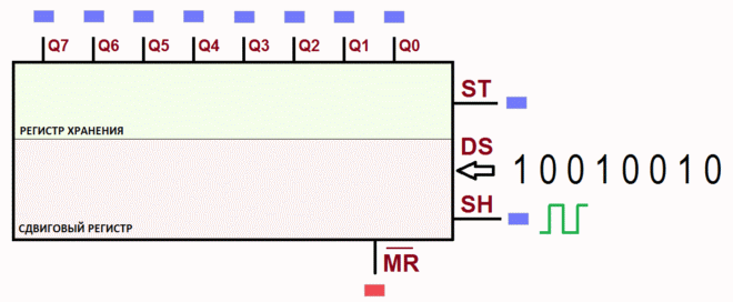
- Q0…Q7– the outputs that we will control. Can be in three states: logical one, logical zero and high-resistance Hi-Z state
- GND- Earth
- Q7′– output intended for serial connection of registers.
- M.R.– register reset.
- SH_CP– input for clock pulses
- ST_CP– data latching input
- O.E.– an input that transforms the outputs from HI-Z into operating state
- D.S.– data input
- VCC– power supply 5 volts
Register logic
When on clock input SH_CP a logical one appears, the bit located at the data input D.S. read and written to the shift register. This bit is written to the least significant bit. When the next high-level pulse arrives at the clock input, the next bit from the data input is written to the shift register. And the bit that was written earlier is shifted one bit to the left, and its place is taken by the newly arrived bit. The next clock pulse will write the third bit, and the previous two will move further. When all eight bits are filled and the ninth clock pulse arrives, the register begins to fill again from the least significant bit and everything repeats again. So that the data appears at the outputs Q0…Q7 you need to “snap” them. To do this, you need to apply a logical one to the input ST_CP.
- M.R. resets the register, setting all outputs Q0…Q7 to a logical zero state. To perform a reset, you need to apply a logical zero to this input and apply a positive pulse to the input ST_CP. A very useful function, since when power is applied to the microcircuit, a certain arbitrary value appears at the output. When working with a register, a logical unit must be located at this pin.
- O.E.(output enable) if a logical 1 is applied here, the outputs will be in a high-resistance HI-Z state. When we apply logical 0 to this input, the outputs will be in working condition.
- Q7′
designed for serial connection of shift registers.
But it’s better to see once than to read twice =) so let’s look at the animation:
Working with the register head-on
When mastering the work with an unfamiliar microcircuit, it is often useful to work head-on, that is, directly twitching the controls with your feet, this allows you to better understand the principles of working with the test subject. So, following the logic of the work, I wrote a program that should output the binary number 10010010 to the register output
$regfile
= "attiny2313.dat"
$crystal
=
1000000
Config
Portb = Output
Sh_cpAlias Portb. 3 "leg for clock pulses
DsAlias Portb. 2 "data output leg
St_cpAlias Portb. 0 "leg for "latching" data into the holding register
"output through the register of the number 146 (in binary representation 10010010)
St_cp=
0
"put your foot in data recording mode
Ds=
1
"set the first bit
Sh_cp=
0
"we give an impulse to the clock output
Sh_cp=
1
Ds=
0
"set the second bit
Sh_cp=
0
Sh_cp=
1
Ds=
0
"set the third bit
Sh_cp=
0
Sh_cp=
1
Ds=
1
"set the fourth bit
Sh_cp=
0
Sh_cp=
1
Ds=
0
"set the fifth bit
Sh_cp=
0
Sh_cp=
1
Ds=
0
"set the sixth bit
Sh_cp=
0
Sh_cp=
1
Ds=
1
"set the seventh bit
Sh_cp=
0
Sh_cp=
1
Ds=
0
"set the eighth bit
Sh_cp=
0
Sh_cp=
1
St_cp=
1
"snap the entered data
End
we compile, embed into the microcontroller or look into the simulator and see our combination at the output.

It works, the sent number appears at the register output!
Working with a register in this way, although possible, is too cumbersome and takes up a lot of program memory. But it clearly demonstrates the entire methodology for working with this microcircuit. Let's consider a more suitable method.
Controlling the 74HC595 register in Bascom using the ShiftOut command
Bascom-AVR has a great team for working with all kinds of serial interfaces SHIFTOUT
This command itself will decompose the number into bit components and sequentially output them to any pin of the microcontroller; at the same time, it can issue clock pulses. Just right for working with shift registers! Command syntax:
SHIFTOUT Datapin, Clockpin, var, option
Datapin – microcontroller port for data output
Clockpin – microcontroller port for outputting clock pulses
Var – data that we want to send to the register
Option – a number from 0 to 3, this parameter selects the order in which data will be entered into the register and the active level on the Clock line at which the bit is written:
option=0 – the most significant bit comes first, Clock active level low
option=1 –
most significant bit comes first, Clock active level high
option=2 –
least significant bit comes first, Clock active level low
option=3 –
least significant bit comes first, Clock active level high
In our case, to work with the 74HC595 register, the option parameter must be set to 1 or 3.
To latch data into a register, use the command PulseOut. This command outputs a pulse to the microcontroller leg with a specified duration. The command configuration looks like this:
Now let's output the number 10010001 (145 in decimal system) to the output of the register connected to the microcontroller according to the above diagram:
$regfile
= "attiny2313.dat"
$crystal
=
1000000
Dim
A AsByte
Config
Portb = Output
A=
145
Gosub
Hc595 "we go to the data sending subroutine
End
Hc595:
"data sending routine
Shiftout
Portb. 2, Portb. 3, A, 1 "send data to the register
Pulseout
Portb, 0, 5 "snap data
Return
Having flashed the microcontroller, you can see a similar picture; the sent combination of bits is set at the output of the shift register.

As you can see, controlling the 74HC595 shift register in Bascom consists of only two lines of code and does not present any difficulties.
Increasing the bit depth